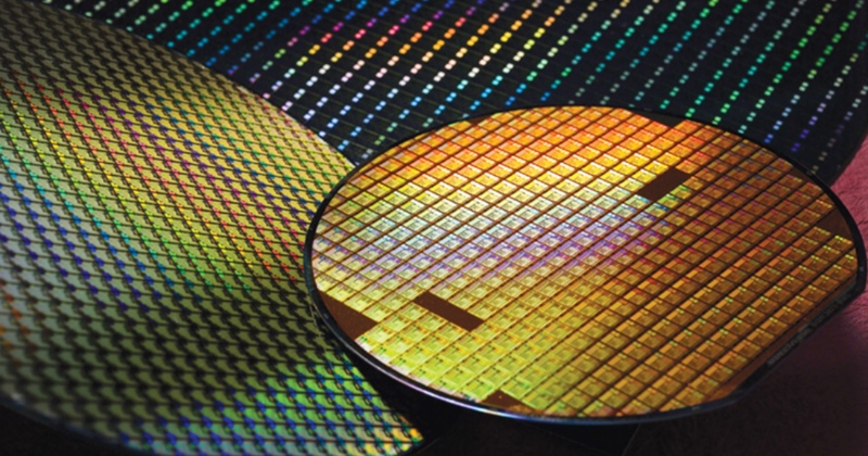
Emerging materials for the semiconductor industry possess a number of unique properties that make them particularly desirable to shrink device geometries and develop novel 3D architectures. Specific material properties include their extreme strength, flexibility, optical transparency and thermal conductivity. While researchers focus an enormous amount of effort on the fabrication and characterization of these materials, integration of these materials into new products and their subsequent industrialization continues to be a challenge. These challenges commonly affect the precision of a required process and repeatable yield of devices as they are industrialized. Useful information to prevent or mitigate these challenges include atomic composition of material or device, influence on transistor device control, chemical properties, and robustness and ease of analysis to deliver clear insight into material properties.
AI Platform
ICURO has launched the industry first AI platform to manage and validate the semiconductor wafer quality in various stages of silicon wafer production applying advanced deep learning techniques.

Intelligent Visual Wizard
It is an user-friendly intelligent platform augmented by visual builder that provides detection and measurement of desirable features in silicon wafers during its manufacturing process with extreme high precision and accuracy by reducing manual steps at every stage in the wafer manufacturing process. The enterprise grade deployable AI applications are best suited for lab and shop floor technicians to augment their visual quality analysis and reduce manual efforts.
ICURO’s visual wizard is for quality engineers, site engineers, production managers. The tool assists the shop floor technicians with an app for rapid Visual inspection for analyzing electron microscope image. The technician will have the following features:
- Create a new project and choose the semiconductor production line association
- Project will have pretrained models related to Yield improvement, Wafer Inspection, Production Optimization
- Load images with dynamic annotation with auto model creation
- Ground truth update for the image analysis
- Summary report for the inference for the entire image analysis for a window of time
End-to-end automation
The intelligent assistant automates the wafer analysis in the semiconductor manufacturing process. The entire pipeline consisting of contour extraction, template matching, and alignment eliminates the manual steps for characterizing semiconductor geometry and features by applying advanced deep learning to automate measurements of wafer microscopy images. The data sources are images from Atomic Force Microscope, Scanning Electron Microscope, and Transmission Electron Microscope. The end-to-end AI pipeline offers both real-time and batch processing for wafer image analysis and measurement of key specifications.

Consumable Model Store for High precision defect detection
Am adaptive AI vision technology is applied for high-precision and recognition of defect areas and simplifies the measurement process on semiconductor wafer electron microscopy images.
ICURO’s ready-to-deploy extensible models include:
- Location and tracking of items for inventory planning and demand forecasting
- Predictive maintenance for anomaly detection in operations coupled with Natural Language Processing based on knowledge graph with Industrial Internet of Things, equipment data.
- Yield in semiconductor manufacturing is key and it is a very time-consuming processes. Provides the ability to identify patterns in component failures, predict likely failures in new designs, and propose optimal layouts to improve yield and also on printed circuit board.
