Advancing Silicon Innovation With Artificial Intelligence

Silicon Everywhere
Silicon is the heart in every aspect of daily life of humans. The emerging mega market trends is seeking a symbiotic ecosystem relationship from silicon to chip and integrated software to innovate products and services. Artificial intelligence (AI) is the key accelerator to realize this market need.
ICURO has made significant investments in developing and deploying AI platforms with applications ranging from design-for-silicon to silicon production process. The silicon functional and technical AI practitioners at ICURO have deployed innovative and integrated platforms and modular systems to transform and realize key outcomes across each and every stage of the silicon value chain.
The Platform Of Platforms For Silicon Innovation
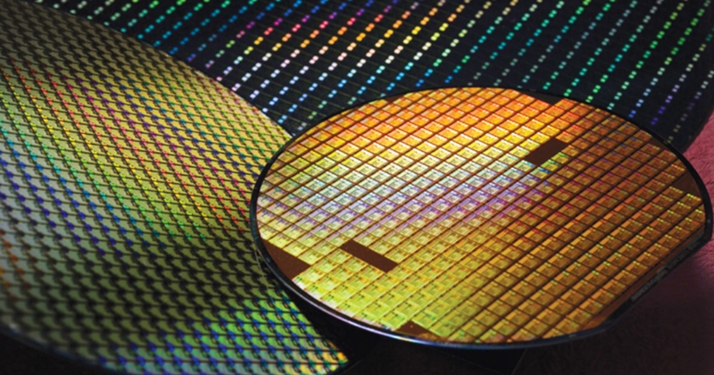
Every chip starts life as a software program before it is fabricated. The processes that transform design code into “sand in the hand” silicon are on the vanguard of chip innovation. ICURO has launched the industry’s first artificial intelligence (AI) platform that adapts to various stages from silicon design to wafer production process by applying deep learning techniques. The only company with functional and technical expertise on the entire silicon innovation lifecycle from silicon design, synthesis to silicon, testing, wafer production, and packaging. Our platform simplifies the integration with silicon design and analysis toolkit, semiconductor manufacturing equipment, lithography, and measurement and testing systems. This platform of platforms has revolutionized the semiconductor production and workforce to leap forward meeting the surging global demand of chips.

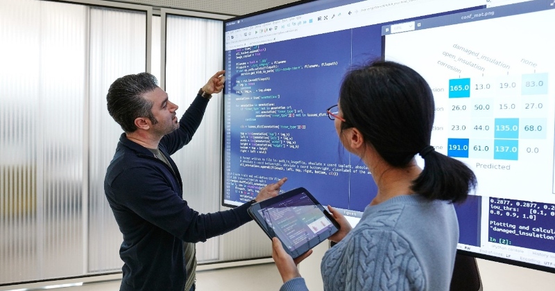
Intelligent Visual Wizard
The no-code AI vision platform with a user-friendly visual builder provides precision analysis and measurement of desirable features in silicon. It is a self-learning AI system embedded in the manufacturing process to deliver extreme high precision and accuracy by eliminating manual steps at every stage of the silicon manufacturing innovation process.
The platform empowers the lab technicians, quality engineers, and production managers with a rapid inline visual analysis and active feedback system to advance yield improvements. Some of the features include the following
- Create a new project and choose the semiconductor production line association
- Platform recommends prebuilt models related to yield improvement, wafer inspection, production optimization
- Load images with dynamic annotation with auto model creation
- Ground truth update for the image analysis
- Summary report of the inference for the entire image analysis

Consumable Multimodal Store
The adaptive AI technology platform integrates with silicon design and analysis toolkit, semiconductor manufacturing equipment, metrology, and visual inspection and measurement subsystems. The adaptive AI techniques remove the extensive labeling of thousands of images or unstructured data that is typically required for a supervised learning pipeline. The production-grade and scalable AI models are best suited for the design lab and shop floor technicians to augment their analysis and reduce manual efforts.
The ready-to-deploy extensible multimodal addresses the following
- Yield in semiconductor manufacturing is key and it is a time-consuming process. AI predicts failure in new designs, identifies patterns in component failures, and recommends optimal layouts to improve yield
- Predictive analytics for anomaly detection in operations coupled with natural language processing based on knowledge graph with industrial IoT, and equipment data
- Location and tracking of items for inventory planning and demand forecasting

End-to-End Pipeline Automation
The intelligent workflow automates every stage from silicon design to semiconductor manufacturing process. It empowers the workforce with digital tools and real time knowledge to adapt, collaborate, and excel in fast-changing conditions. In the wafer manufacturing process, the entire pipeline consisting of contour extraction, template matching, and alignment eliminates the manual steps for characterizing semiconductor geometry and features by applying advanced deep learning to automate measurements of wafer microscopy images. The adapters developed for image capture from atomic force microscope, scanning electron microscope, and transmission electron microscope camera manufacturers. The end-to-end AI pipeline offers both real-time and batch processing for wafer images and measurement of key specifications.

Business Outcomes Driven
Production yield is the key critical success factor in controlling wafer processing costs. It affects output per unit of input resources, waste generation, environmental and financial sustainability, time to market, and costs. Yield improvements provides significant competitive advantages, which are critical in unpredictable economic environments. Production yield improvement can provide cost competitiveness through optimum resource utilization along with waste reduction and achieving sustainable operations. The AI platform has demonstrated consistent business outcomes in the following three critical success factors.
- Implemented systemic yield improvements of 84%
- Delivered high precision vision analytics
- Delivered faster and accurate measurement outcomes
Strategic Partners

Associate Member of SEMI, the global industry association representing semiconductor and electronics manufacturing and design supply chain. ICURO contributes to SEMI Smart Initiatives that advances technology around semiconductors, electronics and imaging systems, the Internet of Things, MEMS, sensors, devices, displays, and other digital technologies used in the electronics industry.
As an Associate Member of SEMI, ICURO is an active innovation partner to the following SEMI Smart Initiatives:
- Smart Data. This initiative aims to improve efficiency in the semiconductor design and manufacturing supply chain through new data analytics, artificial intelligence (AI) and machine learning (ML). In addition to efficiency improvements, activities aim to reduce costs, validate semiconductor chips and products, speed process development and to problem-solve root causes.
- Smart Manufacturing. This initiative focuses on challenges and opportunities integrating production and sensor data, analytics, artificial intelligence, automated systems and more with traditional manufacturing technologies.
- Smart MedTech. Nano-Bio Materials Consortium of SEMI brings critical information and project funding to the electronics industry; the SEMI-FlexTech partnership focuses on the rise of flexible, printed and hybrid electronics to better fit the contours and movement of the human form, in part for healthcare applications.
- Smart Mobility. This initiative is focused primarily on the automotive and autonomous vehicle supply chain. The Global Automotive Advisory Council of SEMI engages stakeholders to address common challenges, priorities, solutions, and opportunities
Strategic Partner of AMD MIVisionX, the comprehensive toolkit consisting of computer vision and machine intelligence libraries, utilities, and applications bundled into a single toolkit. AMD MIVisionX delivers highly optimized conformant open-source implementation of the Khronos OpenVX™ and OpenVX™ Extensions along with Convolution Neural Net Model Compiler & Optimizer supporting ONNX, and Khronos NNEF™ exchange formats. The toolkit allows for rapid prototyping and deployment of optimized computer vision and machine learning inference workloads on a wide range of computer hardware, including small embedded x86 CPUs, APUs, discrete GPUs, and heterogeneous servers.
As a strategic partner, ICURO has been applying AMD Radeon Open Compute (ROCm) and MIVisionX to deliver advanced accelerators to effectively use OpenVX for feature detection and OpenCL for GPU acceleration in Simultaneous Localization and Mapping (SLAM) applications. SLAM is a computational problem for constructing a 3D map of an unknown area while still knowing where the machine or robot exists in the map and this accelerator developed by ICURO is used for a wide range of applications such as 3D perception for machines, robots, and drones.
More in High Tech
Agile Product Innovation
Market leaders in high tech industry are already leveraging artificial intelligence (AI) to achieve unprecedented scale and speed in delivering results. AI enables companies to continuously learn how they can improve processes, enhance partnerships and gauge market forces. Global enterprises in the high tech industry are leveraging AI to reshape three core functions;[…]
High Tech As-A-Service

While digital technology advancements continue to disrupt the high tech industry, the critical success factors in this digital environment is determined by how businesses adapt to these changes. High tech companies that differentiate themselves are the ones that build their products and solutions, digitize channels and streamline business processes based on the needs of their end customers and partners.[…]
Network Maintenance Analytics

Internet of Things (IoT) analytics is the application of data analysis tools and procedures to realize value from the huge volumes of data generated by connected IoT devices. Data integration in a complex network of devices is becoming increasingly challenging for global enterprises. As the number of connected devices grows exponentially, companies are struggling to […]
Implementation Roadmap
Building and delivering an enterprise AI roadmap can divided into a three-step process. Step one begins with strategic goals and opportunity discovery process where AI can enhance, automate, and accelerate. Step two lays out the foundation to define intelligent workflows for key business actions and value realization. Step three brings you closer to a constantly learning enterprise that adapts to business changes and delivers strategic growth outcomes.

Automate
- Value Engineering
- Hybrid Dataflows
- Scalable Operations

Predict
- Intelligent Workflows
- Business Decisions
- Scalable Outcomes

Prescribe
- Explainable AI
- Value Observability
- Business Adaptability